What is a grating coupler?
Grating couplers are periodic lines that are etched into
the top of the waveguide, which re‐direct the light from
the optical fibre into the waveguide.
What is an edge coupler?
An edge coupler is a device that couples light from fibre to the chip using inplane/butt/ edge coupling.
Tapering is a vital component for these devices.
Advantages of edge coupling
Edge coupling, in essence, is the inverse taper method.
- Broad wavelength range
- Low facet reflection
- Easy to fabricate (if you can make tips)
Advantages of grating couplers
- No facet preparation necessary
- Can be fabricated using lithography and etching at the wafer scale, so cheap
- Do not need to be placed at the edge of the chip
- The shape can be matched well to the shape of the fibre mode
Disadvantages of general edge couplers
Relatively incompatible with wafer-level testing
Requires high-quality facets on the chip
Disadvantages of Grating Couplers
- More wavelength-selective than edge couplers
- Fibre must approach chip from the surface (possibly a packaging problem)
Chip Facet Considerations in edge coupling
Chip facet: the chip facet must be made very smooth, to reduce unwanted scattering. This can be done by polishing, cleaving, or dicing…all of which can be expensive processes.
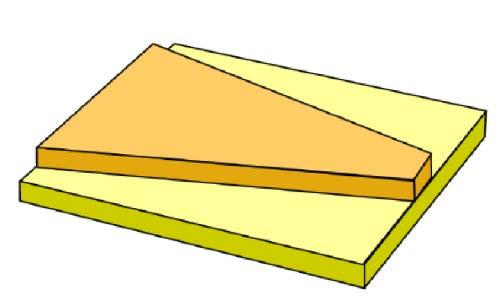
Describe Regular Planar Taper
- Widen the waveguide, with no change in height.
- Still inefficient, due to mode mismatch in height.
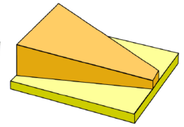
Describe 3D Taper
- Gradually widen the waveguide in width & height, for better mode matching
- This is very difficult to fabricate – a greyscale lithography mask can be used (unusual), and the fabrication process must be well calibrated
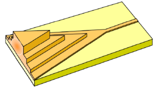
Describe 3D Taper Etch Steps
- Increase the height in steps, requiring only standard lithography steps.
- More lithography steps are needed (more expensive)
- If starting with thick layer and etching down to form waveguide, more scattering loss.
Edge Coupler Consideration
Even if you match the mode shape of the waveguide to the mode shape of the fibre well, if the waveguide effective index is greater than that of the silica glass that the fibre is made of (n=1.45), there will be a reflection at the interface.
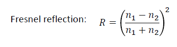
Give Equation for Fresnel Reflection

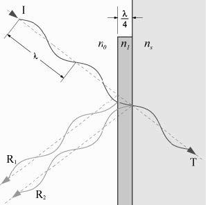
What is an anti-reflection coating?
Thin-film coating, which has a refractive index between that of two materials.
Used to reduce the reflection at the interface of the two optical materials.
How does Rayleigh’s film anti-reflection coating reduce reflection?
To minimise the reflection, the refractive index of the
intermediate layer should be the geometric mean of the
refractive indices of the two outer layers:
Reflection can be further suppressed by including more
layers between waveguides of different widths.
Describe interference Coatings
which also involves inserting a thin film at the interface.
There will be a reflection from the first and second boundaries of
that thin film, which will then interfere with each other. The
thickness of the thin film can be chosen such that they interfere
destructively, minimising the reflections.
For this there should be a 𝜋 phase shift (Δ𝜃) between the two
reflected beams:
Δ𝜃 = (2πn1L)/𝜆
Hence π = (2πn1L)/𝜆
Rearrange, L = 𝜆/2n1
For Normal Incidence, Layer thickness
t = L/2
Therefore t =𝜆/4n1
-
Optical Fibres97
-
Bipolar Junction Transistors24
-
Ring Resonators36
-
MOSFETS36
-
Operating Systems70
-
Assembly73
-
Memory114
-
Coupling16
-
Polarisation4
-
Mask Design Issues2
-
PiC Basics1
-
Splitters And Couplers12
-
Arithmetic27
-
Datapath And Pipelining49
-
Execution2
-
Instruction Sets9
-
Interfacing8
-
Microcoding and Physical Effects1
-
Multicores and Threads1
-
Optimisation20
-
Performance5
-
Toolchains12
-
Lasers4
-
LEDs6
-
Metal Semiconductor Interface0
-
Quantum Wells10
-
Waveguide Loss6
-
MZI16
-
Photovoltaics32
-
MUX16
